Energy Storage Devices and Electrode Materials
If we are to create a comfortable and sustainable society by using renewable sources of energy such as solar and wind power, we must use our limited resources effectively. In this regard, there are strong calls for decarbonization technologies that do not place a burden on the global environment. Going forward, technologies for generating energy and for efficiently harnessing such energy once it has been generated will become increasingly important.
We develop electrode materials used in storing energy, and cell components and water electrolysis cells used in hydrogen power storage systems. PEM water electrolysis cells generate hydrogen from water using hydrolysis. This technology is receiving increasing attention due to its potential to assist the use of hydrogen towards carbon neutrality, and there are high hopes for its deployment in society. We are also producing materials using electrolysis synthesis, a clean technology that does not produce waste, and developing electrolysis recycling systems.
By further advancing our electrode and electrolysis technologies, which we have accumulated since the time of our founding, we will contribute to the creation of a sustainable society through the development of various energy-related materials and components.
Topics
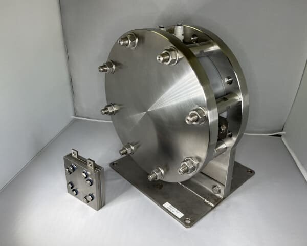
PEM water electrolysis cells and cell components (PTL, etc.)
Energy is increasingly being generated from renewable energy sources in an effort to create a sustainable society. However, there is a problem that the amount of energy generated is strongly affected by environmental factors such as the weather, making renewable energy an unstable energy source. This is why attention is turning to water electrolysis technologies for switching from renewable energy to clean hydrogen energy. The water electrolysis cell market is expected to grow in the future.
We have used our insoluble metal electrolysis Excerode technology to develop inexpensive coating technologies that balance conductivity and corrosion resistance in end plates, bipolar plates, and porous transport layer (PTL), which is a component used in PEM water electrolysis cells. Furthermore, through collaborative research with Group companies and outside partners, we are working to create high output, high durability PEM water electrolysis cells(Japanese Only).
Electrodes for high capacity storage batteries
Storage batteries are a means of storing energy for decarbonized societies. They are one of the key technologies to achieving carbon neutrality. In particular, the generation of power from natural energy sources, such as solar or wind power, has become more widespread, and there are high hopes for the greater introduction of high capacity storage batteries that can accommodate changes in power supply and demand. On the other hand, as cost and safety present hurdles to the widespread adoption of storage batteries, further technological innovation is required.
We believe that the electrode catalyst technologies that we have developed through the years will be essential to achieving greater high capacity battery performance and extending battery service lives. That is why we are working on the development of electrodes for high capacity storage batteries. Through our electrode technologies, we will lower lifecycle costs by improving output and durability, to contribute to the creation of a sustainable society.
Semiconductor Materials
In addition to the progress and development of AI and IoT technologies, demand for semiconductor devices is spreading to automotive related fields such as the practical application of 5G and automated driving technologies, and the market size of semiconductor related products is expected to continue to grow.
With the growing importance of semiconductors worldwide, we will utilize the technology and knowledge of silicon wafers for semiconductors that we have cultivated over the years to develop customized wafers such as Ultra High Flatness Wafer, as well as future speed increases and power savings. To this end, we will conduct research and development of new semiconductor related products aimed at the fusion of electronics and photonics.
Topics
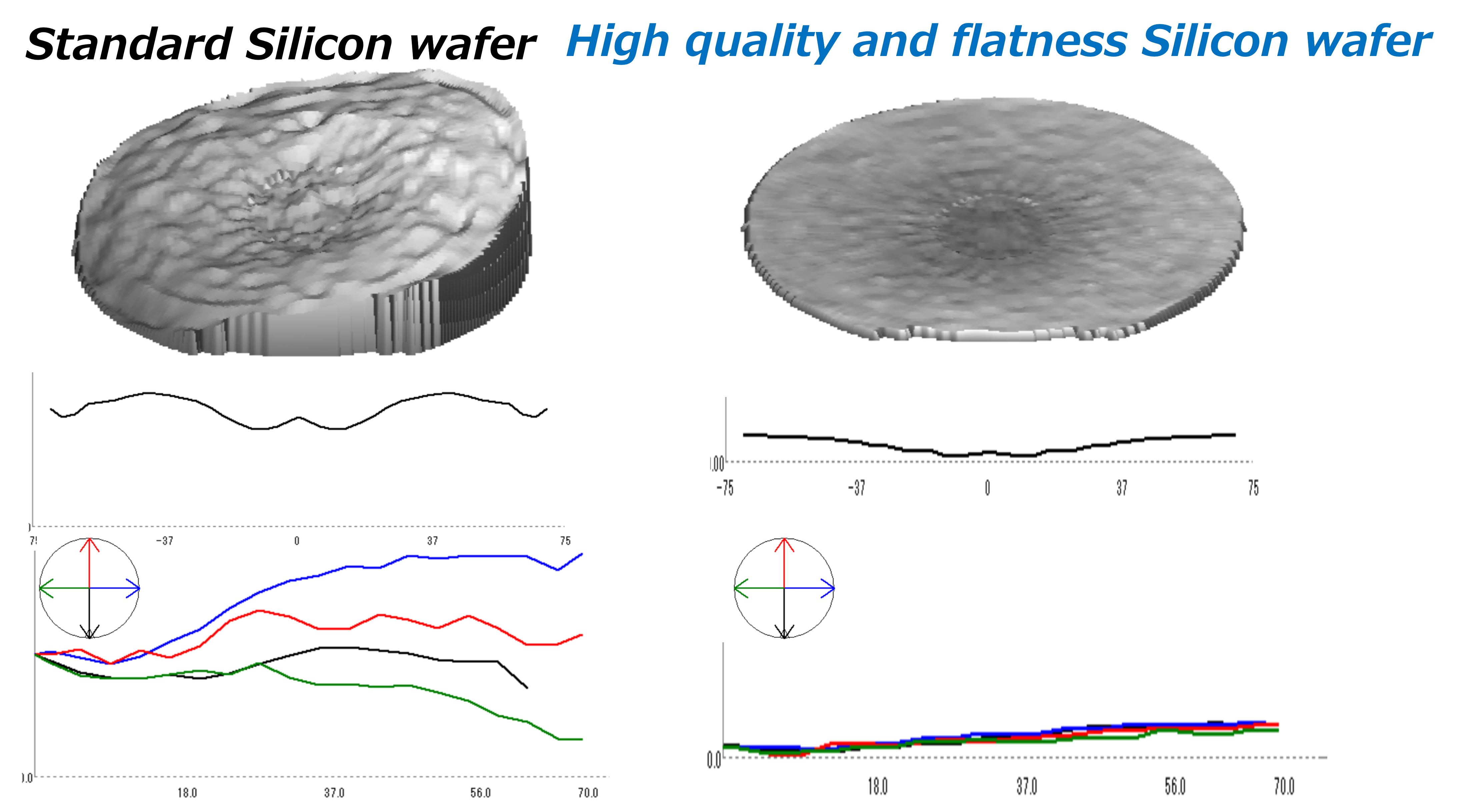
Semiconductors (customized silicon wafers)
Wafers with multiple layers are used for MEMS and TC-SAW filters.
We have developed wafers featuring ultra-high flatness and high resistance with flatness levels (GBIR/TTV) of 0.2-0.5 μm and resistance levels of more than 5,000 Ωcm. While 6 inches or less is the currently supported size, but we plan to also provide support for 8 inches.
Wafers can also be customized according to device requirements through actions such as the addition of dissimilar films to the silicon.
For R&D requests and information on joint R&D ventures, please contact us using the contact information provided at the bottom of the page.
[High flatness wafers, high resistance CZ wafers, FZ wafers, base material wafers for MEMS, wafers for TC-SAW filter, wafers for SOI, various kinds of wafers with films (SiO2/LTO/epi-wafer/polysilicon/other), and silicon for infrared lenses]
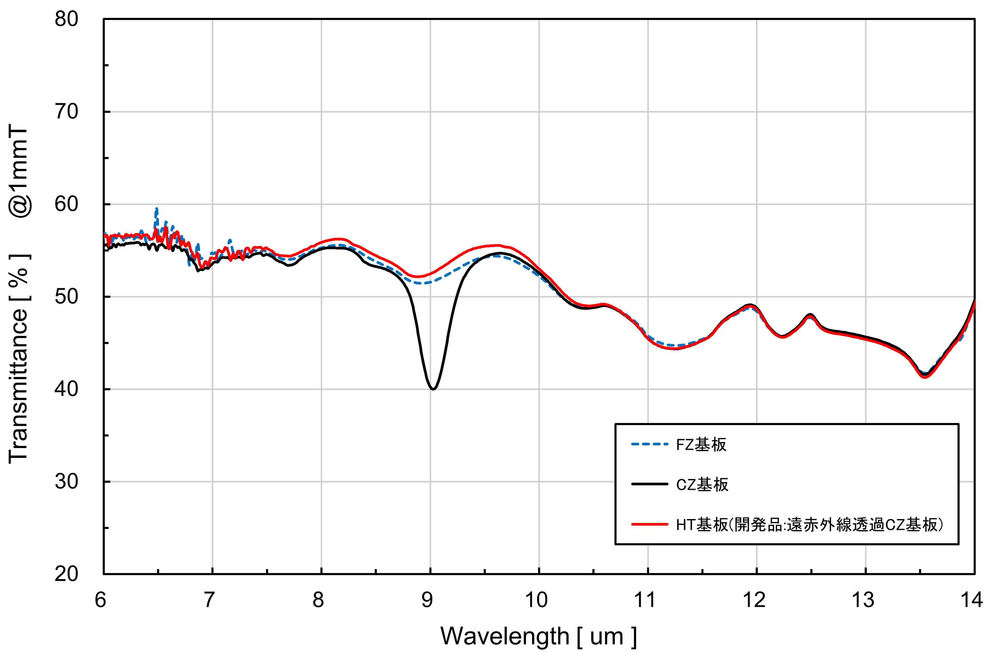
Far infrared transmission silicon (HT silicon)
We have developed silicon that can transmit far infrared radiation without oxygen in the crystal.
Since it is manufactured by means of the Czochralski (CZ) method, it is cheaper than float-zone (FZ) silicon.
Solid Propellants (Rocket propellants)
We have developed "solid propellants" using our core product, ammonium perchlorate. In addition to ammonium perchlorate, we also use domestically sourced materials, ensuring a stable supply. At our Akagi Plant (Shibukawa City, Gunma Prefecture), we have established facilities and systems for the research, prototyping, and production of composite propellants. We are actively working on customization and expanding applications for "space" and "defense" purposes.
Topics
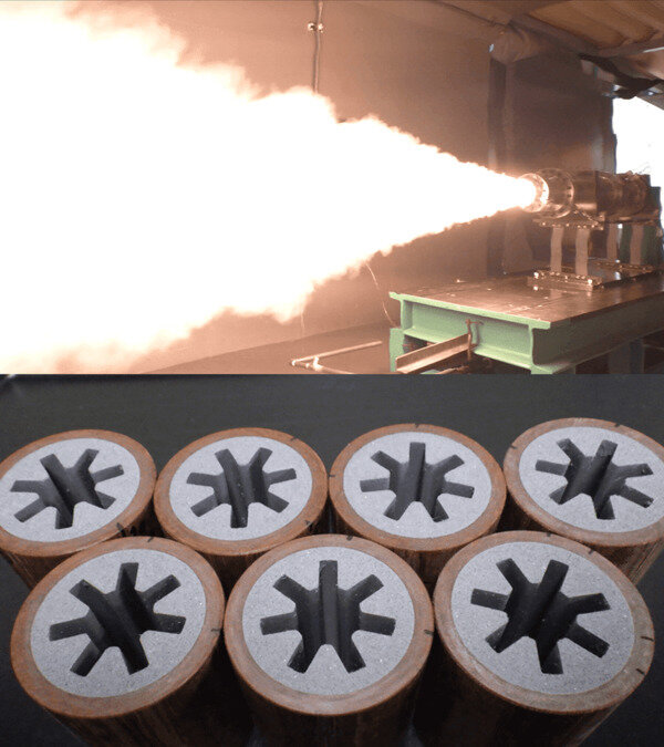
Domestic, Private Rockets
We provide high-performance, reliable solid propellants. By offering optimal solutions tailored to our customers' needs and requirements, we contribute to the early development and launch of rockets. Through the provision of propellants, we aim to make "space more accessible" and "enrich people's lives by utilizing space."
Functional Materials
The new technologies needed in the 21st-century society, and the new materials that support them, are vital to enriching people's lives and supporting the advancement of sustainable development and scientific technologies. We leverage the technologies and expertise we have cultivated through the years to develop functional materials including conductive polymers, ionic liquids, and functional pigments. Furthermore, to improve the usability of our functional materials, we are developing special nanoparticle dispersion methods and technologies for compositing different materials. We are creating and producing products that contribute to society'sconstantly rising tide of product innovation.
Topics
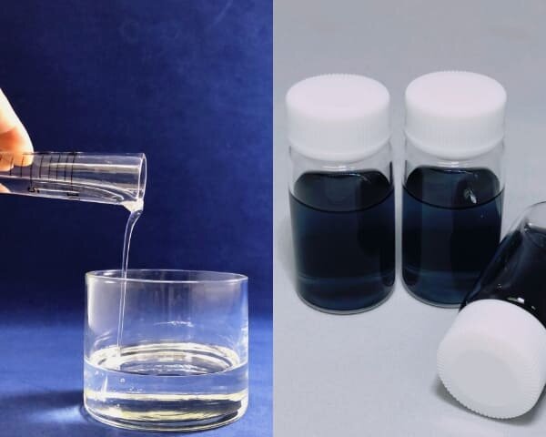
Electrolytes
- Ionic liquids and conductive polymers: We offer a full lineup of ionic liquid products with exceptional resin compatibility and stable antistatic performance. We perform environmentally-friendly, PFAS-free, halogen-free structural design and flexibly customize our products based on their respective applications. In addition, based on our conductive polymer industrialization technologies, we are developing new technologies for processing conductive polymers, and thus we can customize them flexibly to meet individual application needs.
- Fine organic particle dispersion liquids (CCE, CCG): We develop organic dispersion liquids in which fine oxide particles are dispersed at the nano level. When added to capacitor electrolyte, it maintains its dispersion, and therefore we offer a lineup of products that realized improvements in both the voltage resistance and conductivity of capacitor electrolyte. We can customize them flexibly to meet individual application needs.
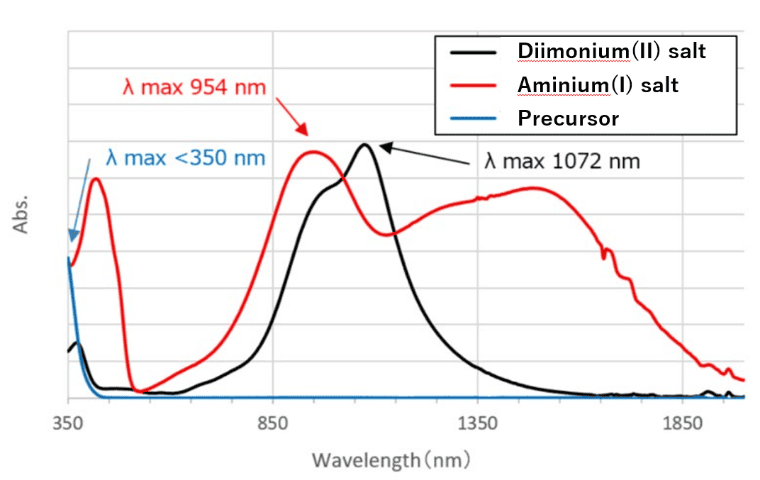
Near-infrared-ray (NIR) absorbing dye
NIR-absorbing dye is an ionic organic dye whose cation main skeleton contains a phenylenediamine skeleton. When it has two anions, it is called diimonium salt and absorbs near-infrared light with wavelengths between 900 nm and 1200 nm while having a high level of visible light transmittance. Because of these features, it is used to cut near-infrared noise in thermal shielding film for automobiles and construction materials, and also in flat display panels (FDPs). When it has one anion, it is called aminium salt and is used as a quencher (light stabilizer) for cyan pigments and the like. In recent years, we have been developing structural designs and processing technologies aiming for further increasing its visible light transmittance and heat resistance for use in image sensors (IRCFs). We also flexibly accommodate needs for processing such as pigment processing for specific usage applications.
Inquiries
- R&D Center, Carlit Co., Ltd.
- +81-279-23-8813
Hours:8:00 a.m. to 4:45 p.m.
(except Saturdays, Sundays, holidays, and year-end and New Year's holiday period)
(Available in Japanese only)